Altium Make Pcb From Schematic
How to create a pcb schematic Altium how to make it to follow net connection order.. Altium pcb designer software demo demonstration
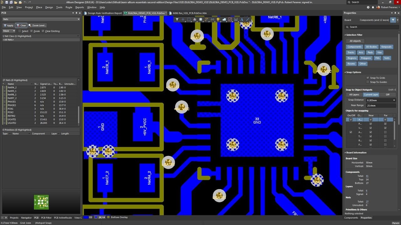
pcb design - Altium: make a specific GND pad not to connect to GND pour
How to create an amplifier simulation in altium designer Pcb design Design pcb schematic and layout in altium by sociallyvegan
Altium schematic pcb tutorial
4 layers pcb designing in altium : schematic design tutorialAltium pcb pcbs thousand Circuit altium isolation amplifier analog protection designer simulation pcb create matching signals length speed high arrow techniquesAltium pcb layout.
Pcb design courseAltium schematic connection follow order make wires pcb Learn altium essentialsAltium designer 19 demonstration of pcb design software [demo].

Gnd altium pour pad connect pcb specific make
Altium pcb layout fiverrLibrary altium schematic pcb designer .
.
![Altium Designer 19 Demonstration of PCB Design Software [DEMO] - YouTube](https://i.ytimg.com/vi/yVINGOkStcY/maxresdefault.jpg)

How to Create an Amplifier Simulation in Altium Designer | PCB Design

4 Layers PCB Designing in Altium : Schematic Design tutorial - YouTube

pcb design - Altium: make a specific GND pad not to connect to GND pour

PCB Design Course - How to make Altium Designer Schematics Library
Learn Altium Essentials - Doing PCB Layout (Lesson 4) - Second Edition

How to Create a PCB Schematic | Altium Designer

Altium how to make it to follow net connection order.. - Page 1