Convert Schematic To Pcb Altium
Pcb guideline altium Design schematic and pcb in altium by wangdegang Design pcb schematic and layout in altium by sociallyvegan
How to Convert schematic diagram into PCB layout in Easyeda Online PCB
Getting started with easyeda part 3: pcb layout How to convert schematic diagram into pcb layout in easyeda online pcb Learning pcb design in one week
Design schematics and pcb in altium by faiz07
Easyeda software presentedAltium fiverr 1 hour tour about altium designer(schematic-pcb designing)Altium schematic pembuatan lanjut langkah tahap selanjutnya bagain cari.
How to create a pcb layout from a schematic in altium designerAltium pcb learning week schematic monitors both complete left board Simple project pcb altium schematic & board ~ filabHow to convert pcb to schematic diagram?.
![Design schematics and pcb in altium by Faiz07 | Fiverr](https://i2.wp.com/fiverr-res.cloudinary.com/images/t_smartwm/t_main1,q_auto,f_auto,q_auto,f_auto/attachments/delivery/asset/042714782a81a45d93d3005cfceb1748-1595361908/Circuit_bb/design-schematics-in-altium-designer.png)
Altium schematics fiverr screen
Altium pcb schematic screen fiverrPcb schematic diagram layout easyeda convert into .
.
![Learning PCB design in one week - We have the Technology](https://3.bp.blogspot.com/-tXDsAiUak0I/V8imfTudvSI/AAAAAAAACuE/Mgq8bAFCavkK8y4AuwFOS22MJbepVNHcwCLcB/s1600/boards.jpg)
![Design pcb schematic and layout in altium by Sociallyvegan | Fiverr](https://i2.wp.com/fiverr-res.cloudinary.com/images/t_main1,q_auto,f_auto,q_auto,f_auto/gigs/112772182/original/cdf53d2ab648887349485ac23951c0adc512adab/design-pcb-schematic-and-layout-in-altium.jpg)
Design pcb schematic and layout in altium by Sociallyvegan | Fiverr
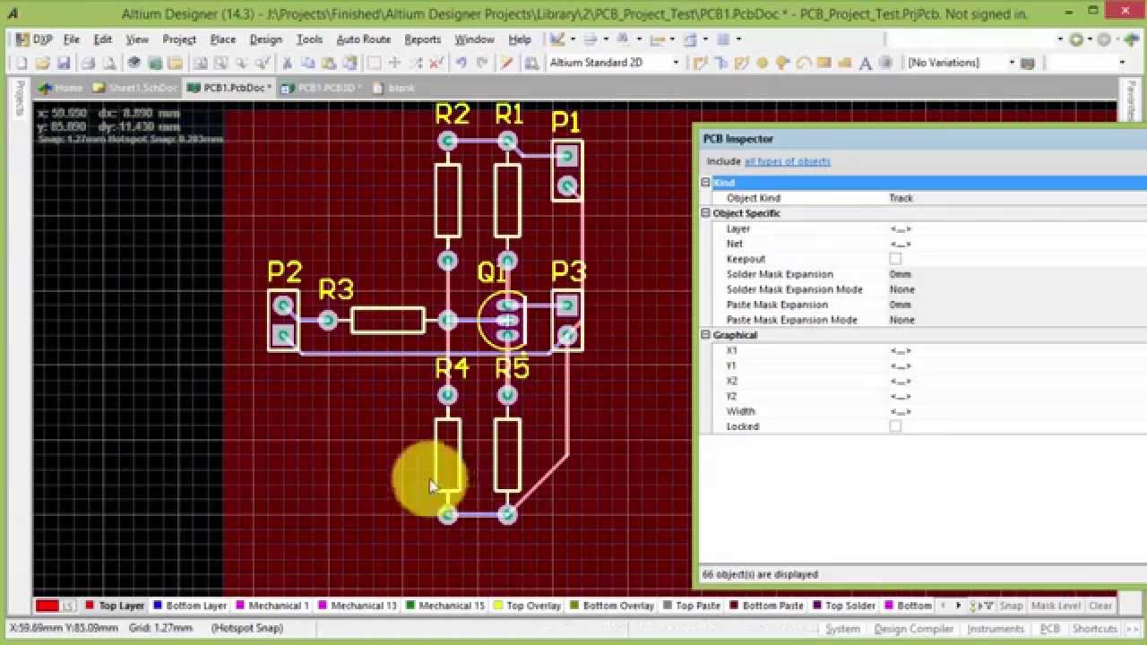
How to Create a PCB Layout from a Schematic in Altium Designer | PCB
![1 Hour Tour about Altium Designer(Schematic-PCB Designing) - YouTube](https://i.ytimg.com/vi/GBk0q3IofNI/maxresdefault.jpg)
1 Hour Tour about Altium Designer(Schematic-PCB Designing) - YouTube
![How to Convert schematic diagram into PCB layout in Easyeda Online PCB](https://i.ytimg.com/vi/aLHUSPz_01Y/maxresdefault.jpg)
How to Convert schematic diagram into PCB layout in Easyeda Online PCB
![How to Convert PCB to Schematic Diagram? - RAYPCB](https://i2.wp.com/www.raypcb.com/wp-content/uploads/2021/03/5f91a49f55206fb.jpg)
How to Convert PCB to Schematic Diagram? - RAYPCB
![Design schematic and pcb in altium by Wangdegang | Fiverr](https://i2.wp.com/fiverr-res.cloudinary.com/images/t_main1,q_auto,f_auto,q_auto,f_auto/gigs/181005974/original/40bd490e13f0e0cf055bfb7f4d3bfdfa958486c7/design-schematic-and-pcb-in-altium.png)
Design schematic and pcb in altium by Wangdegang | Fiverr
![Getting Started with EasyEDA Part 3: PCB Layout - Shawn Hymel](https://i2.wp.com/shawnhymel.com/wp-content/uploads/2016/03/EasyEDA_42.png)
Getting Started with EasyEDA Part 3: PCB Layout - Shawn Hymel
![Simple Project PCB Altium Schematic & Board ~ FILAB](https://3.bp.blogspot.com/-ZHNiMuth7Q4/V1TfLfhMcqI/AAAAAAAADL4/VD-v6pwYZ_8goc5riUWFdHqw-EdQ3ZWMwCLcB/s1600/ss.png)
Simple Project PCB Altium Schematic & Board ~ FILAB