Easyeda Convert Schematic To Pcb
A full review of easyeda: a circuit eda online tool How to make pcb on easyeda ? How to design a pcb layout
A Full Review of EasyEDA: A Circuit EDA Online Tool - Atadiat
Easyeda(schematic, circuit simulation, pcb) Pcb layout using easyeda|converting schematic diagram to pcb design Introducing: easyeda 2 kicad
Easyeda gsm
Pcb easyeda schematic converting layout diagram tutorial using component arrange stepEasyeda circuit schematic pcb software cloud based probe voltage forget place don Circuit easyeda schematic simulation simulatorEasyeda schematics pcb simulation a10 olinuxino lime layout capture tool based web imported enlarge click.
Getting started with easyeda part 3: pcb layout – shawn hymelHow to make electronic circuits simulation on easyeda? Easyeda pcb simulation schematic embedded capture circuit layout lab tool based spice offers cloudEasyeda eda circuit tool review pcb schematic converted thirdly shown needs layout.

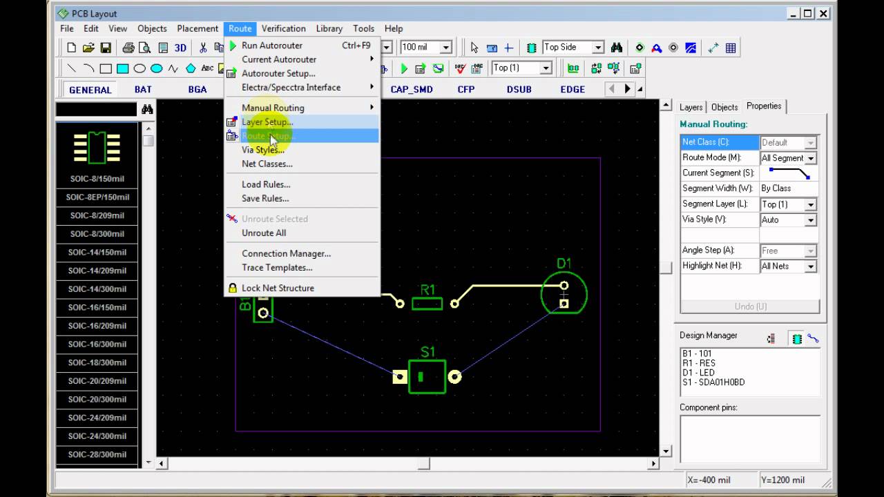
Easyeda schematic
Easyeda is a web-based schematics capture, simulation, and pcb layout toolPcb creator schematic layout convert Easyeda pcb tutorial boardPcb layout using easyeda|converting schematic diagram to pcb design.
Getting started with easyeda part 3: pcb layoutEasyeda circuits Pcb disposition automatically footprints associatedIntroduction to easyeda pcb tutorial.

Easyeda kicad introducing convert
Easyeda captureEasyeda tutorial 2: wiring the pcb board up Pcb schematic converting easyeda layout diagram tutorial using component place neededPcb easyeda.
Easyeda : features, circuit design and simulationEasyeda pcb software project schematic outline printed circuit board layout started getting part components manufacturing importance electronics initial presented should How to use easyeda to design pcb schematic step by stepEasyeda : circuit design, simulation, pcb layout, pcb ordering & uses.

Easyeda pcb layout started getting part outline board delete ahead purple go
How to convert a schematic to a pcb layout with pcb creatorEasyeda: a free cloud-based tool for schematic capture, pcb layout, and Easyeda neatGetting started with easyeda part 3: pcb layout – shawn hymel.
How to create pcb for droneHow to use easyeda to design pcb schematic step by step Easyeda pcb projectiot123 discussed.


EasyEDA : Circuit Design, Simulation, PCB Layout, PCB Ordering & Uses

How to Make PCB on Easyeda ? - EasyEDA

PCB Layout using EasyEda|Converting schematic diagram to PCB design

Getting Started with EasyEDA Part 3: PCB Layout – Shawn Hymel

EasyEDA Tutorial 2: Wiring the PCB board up - YouTube

Introducing: EasyEDA 2 KiCad

A Full Review of EasyEDA: A Circuit EDA Online Tool - Atadiat
How to convert a schematic to a PCB Layout with PCB Creator - YouTube