Kicad Highlight Net Schematic
Highlight net when routing Kicad schematics Kicad info
Schematics Capture and PCB Layout in Linux with Kicad - CNX Software
Highlight kicad pcbnew eeschema info kb shot screen Highlight a net in legacy, something simple (solved) Kicad routing 1026
Kicad schematics tutorial
Kicad schematics pcb capture software a10 allwinner cnx orcad linux layoutKicad schematic schematics Kicad edaKicad schematic.
Kicad schematics tutorialKicad schematics tutorial Kicad eda symbol hackrfKicad tutorial.
![Ability to highlight related nets - Layout - KiCad.info Forums](https://i2.wp.com/forum.kicad.info/uploads/short-url/pJNo4qJhON6vkH4yEpDfgQAlc6R.png?dl=1)
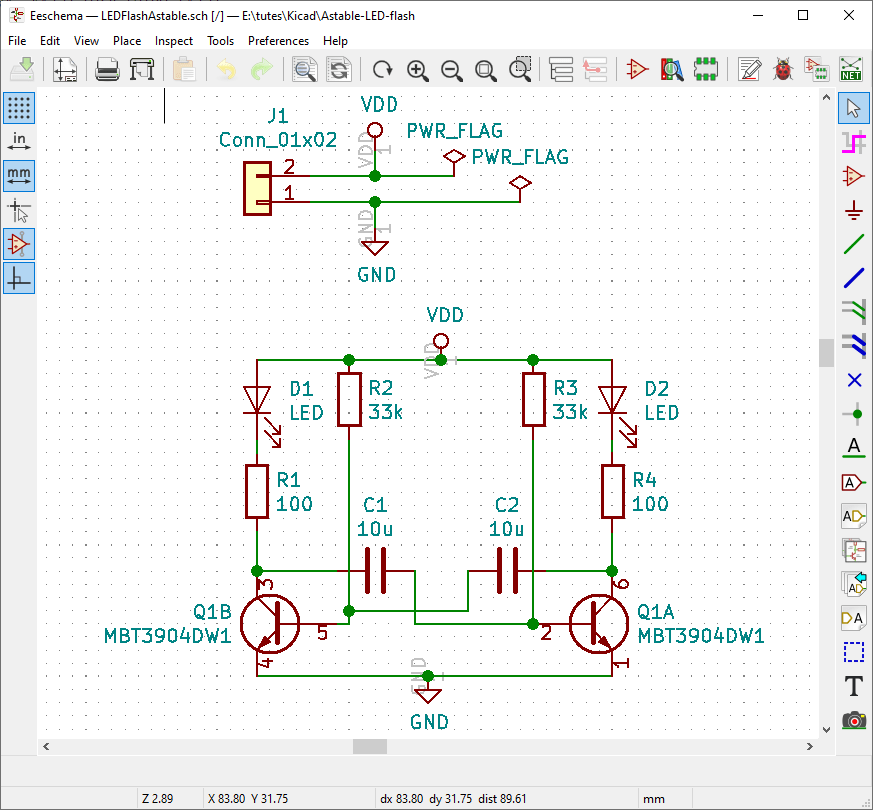
Schematics capture and pcb layout in linux with kicad
Kicad connecting two nets [solved]Kicad schematics Achievement unlocked: schematics converted to kicad and posted onAbility to highlight related nets.
Kicad pcb schematic component footprints assign select tools menu firstDesign a schematic in kicad by ukelectronics Kicad schematics ledsSolved kicad.
![Week 11](https://i2.wp.com/fabacademy.org/2019/labs/lakazlab/students/abdoelaziz-shafier/img/week11/schematica.png)
Highlight net in pcbnew from eeschema
Ability nets kicad 1040 .
.
![Schematics Capture and PCB Layout in Linux with Kicad - CNX Software](https://i2.wp.com/www.cnx-software.com/wp-content/uploads/2012/05/kicad_schematics_eeschema.jpg)
![Achievement Unlocked: Schematics Converted to Kicad and Posted on](https://i2.wp.com/propeddle.com/wp-content/uploads/2014/02/propeddle-kicad.png)
Achievement Unlocked: Schematics Converted to Kicad and Posted on
![Highlight net in pcbnew from eeschema - Layout - KiCad.info Forums](https://i2.wp.com/kicad-info.s3.dualstack.us-west-2.amazonaws.com/original/2X/e/e2a5c7d19a63bee088adaa152ea52faeb2d56819.png)
Highlight net in pcbnew from eeschema - Layout - KiCad.info Forums
![KiCAD Connecting Two Nets [SOLVED] - Schematic - KiCad.info Forums](https://i2.wp.com/kicad-info.s3.dualstack.us-west-2.amazonaws.com/optimized/3X/1/7/17e659393cc7c218fafc76729b2d8589956b110f_2_1024x514.png)
KiCAD Connecting Two Nets [SOLVED] - Schematic - KiCad.info Forums
![Design a schematic in kicad by Ukelectronics](https://i2.wp.com/fiverr-res.cloudinary.com/images/t_main1,q_auto,f_auto/gigs/112613308/original/87825b99877f8289c4d3b9f17b3bddff0416e790/design-a-schematic-in-kicad.png)
Design a schematic in kicad by Ukelectronics
![KICAD Schematics Tutorial | Direkt Embedded](https://i2.wp.com/www.direktembedded.com/wp-content/uploads/2021/05/image-2.png)
KICAD Schematics Tutorial | Direkt Embedded
![KICAD Schematics Tutorial | Direkt Embedded](https://i2.wp.com/www.direktembedded.com/wp-content/uploads/2021/05/image-23.png)
KICAD Schematics Tutorial | Direkt Embedded
![KiCad - Schematic to PCB - Manchester HacSpace - Laser PCB](https://i2.wp.com/hacmanchester.github.io/LaserCutter.PCB.Making/images/KiCad/SchematicPCB/Schematic2.png)
KiCad - Schematic to PCB - Manchester HacSpace - Laser PCB
![KiCad EDA - Schematic Capture & PCB Design Software](https://i2.wp.com/www.kicad.org/img/frontpage/kicad_eeschema.png)
KiCad EDA - Schematic Capture & PCB Design Software
![Highlight a net in legacy, Something simple (solved) - Layout - KiCad](https://i2.wp.com/forum.kicad.info/uploads/short-url/grXsv46BoSHIycUJq3OTJdPVPd.png?dl=1)
Highlight a net in legacy, Something simple (solved) - Layout - KiCad